前のページ 次のページ
Mx FFC 15466 2.20-0.55 mate/w 505278-1070 錫
30 cycles: F31S F31W F31L
Amp 10051922-1010ELF 下 💵0.46 9個⭕️
HRS FH34D-8S-0.5SH(50) 8P 💵0.22 5k
Mx 5034801000 上下 D3.6 W6.7 H1.0 💵0.28
TE 1-2328702-0 BkFlip 💵0.193 8Pも安い❤️
上下 D3.83 W7.0 H1.0 ピンヒンジ👍
OMRON XF3M-1015-1B 💵0.36 在庫1 上下
XF2M-1015-1A 上下 D5.9 W9.1 H2.1 💵0.50 1k
59453-081110EDHLF ピンヒンジ💪 8P💵0.64
Mx 505110-1092 FrFlip D5.3 💵0.20 ⭕️9k個
HRS FH12-10S-0.5SH(55) FF 🟡 💵0.48
HRS FH28-10S-0.5SH(05) FF 💵0.35
H2.55W9.9D7.2 保持力2倍 FH12比💪
HRS FH52-10S-0.5SH FF H2.0W9.3D5.7 💵0.28
HRS FH52E-10S-0.5SH FF 💵0.34
Amp F31L-1A7H1-11010 強保持 30cy 在庫3 見積中
GCT FFC2B35-10-T D6.8 W9.4 H2.0 💴42@M
Molex 527451096 RA D4.3 上接点 スライド
527451097 🟡 💵0.76
527450897 8pos 🟡 💵0.34 ⭕️
Molex 527461070 RA D4.3 スライド
527461071 🟡Gold 💵0.24 ⭕️1k個
Molex 525591052 🟡 💵0.59 H3.9 ⭕️
HRS FH12-10S-0.5SVA(54) Flip 💵0.72 H4.85
GCT FFC2A32-10-T Slide H4.3 💵0.38
Amp F31S-1A7L1-11010 Flip H5.8 💵0.54 32個
Dual contact, 強保持 20gf/pin, 🟡
Amp F31W-1A7H1-11010 Slide 💵0.59 13個
GCT FFC2A36-10-0-T Flip H5.2 💴56@M
NDK NX3225GA-12MHZ-STD-CRG-2 💵0.25
YXC X322512MOB4SI 12p 💵0.073
YXC X322512MMB4SI 10p 💵0.087
YXC X322512MSB4SI 20p ✅Basic
TXC 7M12000146 10p 💵0.16⭕️
TXC 7V12000005 10p 黒 💵0.16🪨
TAITIEN XXCBELNANF-12M 10p 💵0.143
SJK 7U12000E12UCG 12p 刻印🌟 💵0.10
#
https://www.downtowndougbrown.com/2024/06/fixing-a-knockoff-altera-usb-blaster-that-never-worked/
ダグ・ブラウン@ 2024-06-09 13:32
1 つ指摘しておきたいのは、さらにテストを行った結果、この投稿で修正したどちらのクローン デバイスでも、Altera/Intel のプログラミング ソフトウェアの新しいバージョンは動作しないようです。
ダグ・ブラウン@ 2024-06-09 15:56
さらにテストを進めた結果、これらの安価なUSB Blaster 2つ(少なくとも私が使っているMAX 10 FPGAとの組み合わせ)でLinuxとWindowsの両方で正常に動作する最後のバージョンは20.1.1であることがわかりました。Intelによると、MAX 10の最終サポートバージョンは21.1とのことですが、私の環境では21.1で「進捗状況が4%で止まる」問題が発生しています。これは安価なクローン製品との非互換性ではなく、Quartusソフトウェアのデバイスサポートの問題である可能性があります。確実に確かめるには、より新しいFPGAをプログラミングするか、より高価な正規のUSB Blasterを購入する必要があるでしょう。
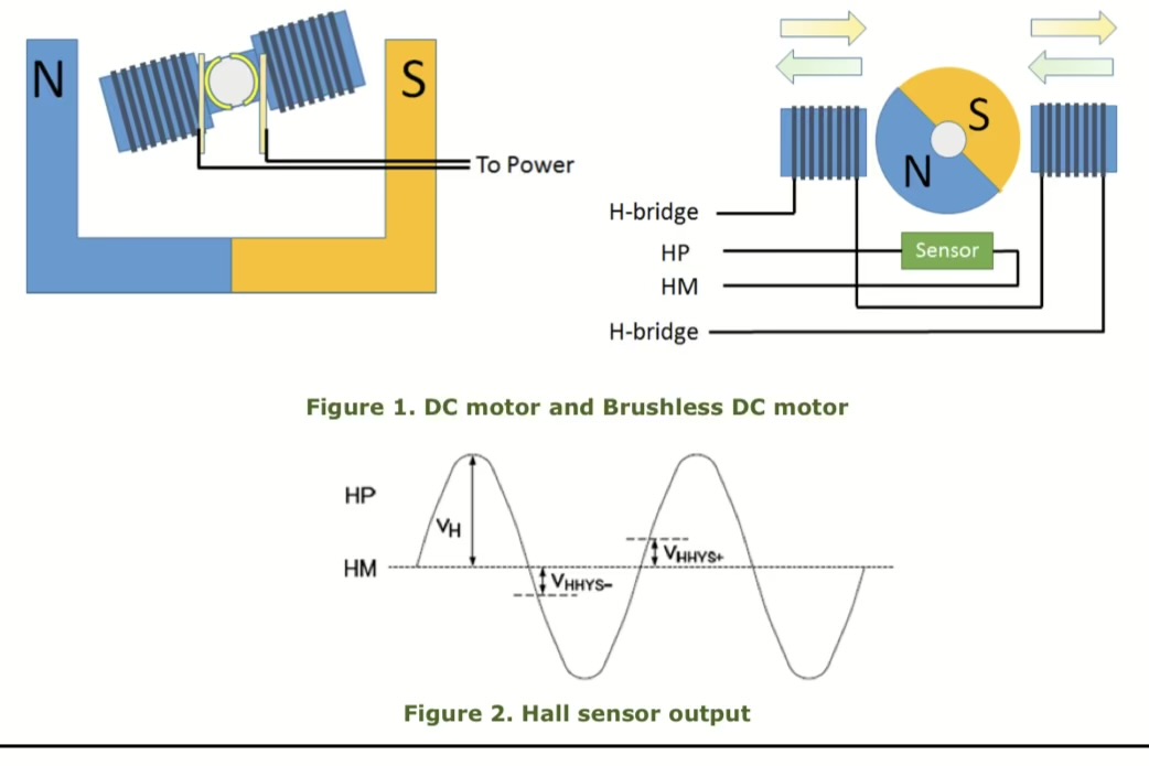
DCモーターは近年ますます頻繁に使用されるようになり、コントローラーハードウェアと駆動方法論の継続的な改善による効率性の利点が増大しているため、従来のACモーターに取って代わるケースが多くなっています。
MachXO2には、FPGAリソースを制御するために使用されるフィーチャー行が含まれています。例えば、フィーチャー行はMachXO2のSRAM構成メモリのロード方法を決定するために使用されます。他のFPGAでは、この操作は外部I/Oピンを使用して制御されます。フィーチャー行は、構成可能な機能の選択においてより高い柔軟性を提供し、デバイス上で利用可能なI/Oの数を増やし、ハードウェアの変更を不要にします。
現場での変更は想定されておらず、開発専用です。
機能行設定の変更により、アクティブな構成ポートが利用できなくなる可能性があります。
Diamond Programmer または Diamond Spreadsheet View を使用して変更可能です。
フラッシュ更新時に消去され再プログラムされるため、機能行の内容は一貫性を保ってください。
MachXO2のコンフィギュレーションSRAMメモリには、FPGAが動作する前に有効なコンフィギュレーションデータをロードする必要があります。
使用しないポートは無効化(DISABLE)する必要があります。これにはDiamond Spreadsheet Viewの[Global]設定タブで設定できます。各コンフィギュレーションポートはsysCONFIGオプションツリーにリストされます。
外部ロジックがデバイスプログラミングに干渉しないようにする必要があります。MachXO2がFeature Row HW Default Mode状態にある際に、復元されたsysCONFIGピンがアサートされないことを確認してください。一例として、MachXO2がFeature Row HW Default Mode状態になった後にPROGRAMNをアクティブロー信号で駆動することが挙げられます。PROGRAMNを無効化した状態でフィーチャー列の再プログラミングに失敗すると、FPGAのコンフィギュレーションおよびユーザーモード移行が妨げられます。
JTAGENBを使用してJTAGポートを選択的に有効/無効化する際は注意が必要です。JTAG I/Oに接続された外部ロジックは、JTAGプログラミングポートと競合してはなりません。
表5.7は共有sysCONFIGピンのデフォルト状態を示します。ご覧の通り、デフォルトモードのフィーチャー列デバイスでは、JTAG、SPIスレーブ、I2Cポートが有効化されています。MachXO2がユーザーモードに移行すると、SSPIおよびI2C sysCONFIGピンのデフォルト状態は汎用I/Oとなります。これは、デフォルトのsysCONFIGポート設定を使用する場合、SSPIまたはI2Cを用いたMachXO2のプログラミング機能が失われることを意味します。ユーザーモードでSSPIまたはI2C sysCONFIGピンを維持するには、
デバイスがJTAG経由でプログラミング中の場合、JTAGモードプログラミングシーケンス完了までPROGRAMNは無視されます。
デバイス構成中にPROGRAMNピンをトグルすると、プロセスが中断され構成サイクルが再起動します。デバイス設定中はPROGRAMNピンを非アサート状態(High保持)にしてください。
機能行ハードウェアデフォルトモード状態のデバイスでPROGRAMNをアサートすると、SSPIおよびI2Cポートが無効化されます。PROGRAMNを非アサート状態にしてからSSPIまたはI2Cプログラミング操作を開始してください。
PROGRAMNは、汎用I/Oとして予約されている場合でも、電源投入時にアクティブです。PROGRAMNに接続された入力信号が、VCC(min)からINITN立ち上がり時間を超える周波数でハイからローに遷移しないようにしてください。PROGRAMNのハイからローへの頻繁なアサートは、MachXO2の構成を妨げ、FPGAが継続的なRESET状態に留まる原因となります。図5.5を参照。
フィーチャー行が消去または再プログラムされる際は、GPIOとして復旧した場合でもPROGRAMNを必ずディアサートする必要があります。アサートされたままの場合、コンフィギュレーションが正常に完了しない可能性があります。
FPGA-TN-02155-4.8 January 2025
MachXO2™はSRAMベースのプログラマブルロジックデバイスであり、内蔵フラッシュメモリを備えることでMachXO2を不揮発性デバイスとして機能させます。MachXO2はFPGAのプログラミングおよび設定のための豊富な機能セットを提供します。
Key programming and configuration features of MachXO2 devices are:
1149.1 JTAG
Self-download
Slave SPI
Master SPI
Dual Boot
I2C
WISHBONE bus
• BIT – BITファイルは、外部SPIフラッシュに保存されるMachXO2のコンフィギュレーションデータです。これはバイナリファイルであり、変更なしでSPIフラッシュに書き込まれます。
MachXO2デバイスには、SRAMとフラッシュメモリの2種類のメモリが搭載されています。SRAMメモリにはアクティブ構成データが格納されており、これは本質的にFPGAの動作を定義する「ヒューズ」に相当します。アクティブ構成データは、ほとんどの場合、不揮発性メモリから読み出されます。不揮発性メモリは、FPGAのSRAMにロードされる構成データを保持します。
Prior to becoming operational, the FPGA goes through a sequence of states, including initialization, configuration and
tINITL時間期間が経過する
PROGRAMNピンがディアサートされる
INITNピンが外部マスターによってローアサートされなくなった
専用INITNピンは初期化フェーズ中に2つの機能を提供します。第一に、FPGAが現在コンフィギュレーションSRAMをクリア中であることを示すこと。第二に、初期化状態からコンフィギュレーション状態への遷移を防止する入力として機能することです。
Assertion of the PROGRAMN input
Cycling power to the MachXO2
Sending the Refresh command using a configuration port
Invoking one of these methods causes the MachXO2 to drive INITN and DONE low. The MachXO2 enters the
オフラインプログラミング – この方法では、デバイスがプログラミングモードに入る必要があります。プログラミングモードでは、プログラミングが完了するまでデバイスは動作を停止します。Diamond Programmerを使用する場合、FLASHで始まる操作でオフラインモードを選択します。操作で特に指定がない限り、アクセスされるフラッシュセクタはFeature、Configuration、UFMです。
バックグラウンドプログラミング – この方法では、デバイスがユーザーモードで動作を継続しながら、構成ロジックがオンチップフラッシュメモリをプログラミングします。オンチップフラッシュメモリのプログラミングが完了すると、デバイスはREFRESH命令でSRAMにダウンロードできます。Diamond Programmer使用時、
バックグラウンドモードはXFLASHで始まる操作で選択されます。操作で特に指定がない限り、アクセスされるフラッシュセクタは
前のページ 次のページ